Introduction
Printed Circuit Board Assembly (PCBA) is the process of soldering electronic components onto a bare printed circuit board (PCB) to create a fully functional electronic assembly. While a bare PCB is just an empty substrate of copper traces and laminate, a PCBA is a working electronic module ready for integration into a final product. At Linked Electronics Co., Limited, we manufacture both bare PCBs and complete PCBA assemblies in-house, giving customers a single source for the full electronics manufacturing workflow — from Gerber file review to a finished, tested board.
This guide walks through the complete PCBA process step by step, the equipment involved at each stage, and the most common questions engineers and procurement teams ask before placing a PCBA order. Whether you are designing your first prototype or scaling to mass production, understanding each step of the PCBA workflow helps you specify your requirements accurately and avoid costly rework.
PCB vs. PCBA: What's the Difference?
The terms are often used interchangeably, but they describe two different stages of electronic manufacturing.
- PCB (Printed Circuit Board): the bare board itself — copper traces, solder mask, silkscreen, and surface finish, but no components mounted. It is an inert substrate.
- PCBA (Printed Circuit Board Assembly): the assembled board — a PCB populated with resistors, capacitors, integrated circuits, connectors, and other components, soldered into place and tested.
A typical electronics product needs both: a manufacturer fabricates the PCB, then assembles it into a PCBA. Linked Electronics Co., Limited offers both services as a turnkey package, eliminating coordination headaches between separate PCB and assembly vendors.
The PCBA Manufacturing Process: 7 Key Steps
A modern surface-mount PCBA line at Linked Electronics Co., Limited follows seven main stages. Each step has specific equipment, quality checks, and design considerations.
Step 1 — Gerber and BOM Review
Before any solder paste hits the board, our engineering team performs a Design for Manufacturability (DFM) review on the customer's Gerber files, bill of materials (BOM), and centroid (pick-and-place) data. We look for issues that could cause assembly defects later: pad sizes that conflict with chosen components, missing thermal reliefs, footprint orientation errors, unavailable parts, and unclear component polarity.
At Linked Electronics Co., Limited, this review is included in every PCBA quote and typically completed within 24 hours of file submission. Catching an issue at the DFM stage costs minutes; catching it after the first article assembly costs days and money.
Step 2 — Solder Paste Printing
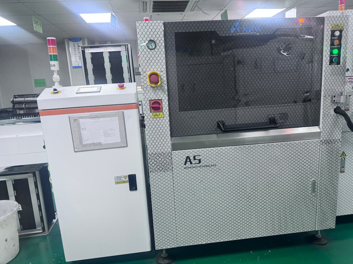
The first physical step of PCBA is depositing solder paste onto the PCB's surface-mount pads. A stainless steel stencil — laser-cut with apertures matching every SMD pad — is aligned over the bare board. A squeegee then drags solder paste across the stencil, forcing precisely metered amounts of paste through the apertures and onto each pad.
Paste volume, alignment, and consistency are critical. Too little paste causes open joints; too much causes bridging between adjacent pads. Linked Electronics Co., Limited uses automatic solder paste inspection (SPI) on production runs to verify paste deposition before the board moves downstream.
Step 3 — Pick and Place
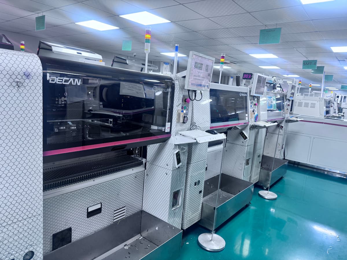
With paste in place, the board enters a high-speed pick-and-place machine. Components are loaded onto the machine on reels, trays, or sticks. A camera-guided vacuum nozzle picks up each component, verifies orientation against the centroid file, and places it onto its corresponding paste-printed pad with placement accuracy down to ±0.03 mm.
At Linked Electronics Co., Limited, we routinely handle components from 0201 chip resistors up to large BGAs, QFNs, and connectors. The pick-and-place machines are programmed directly from the customer's BOM and centroid data prepared during Step 1.
Step 4 — Reflow Soldering
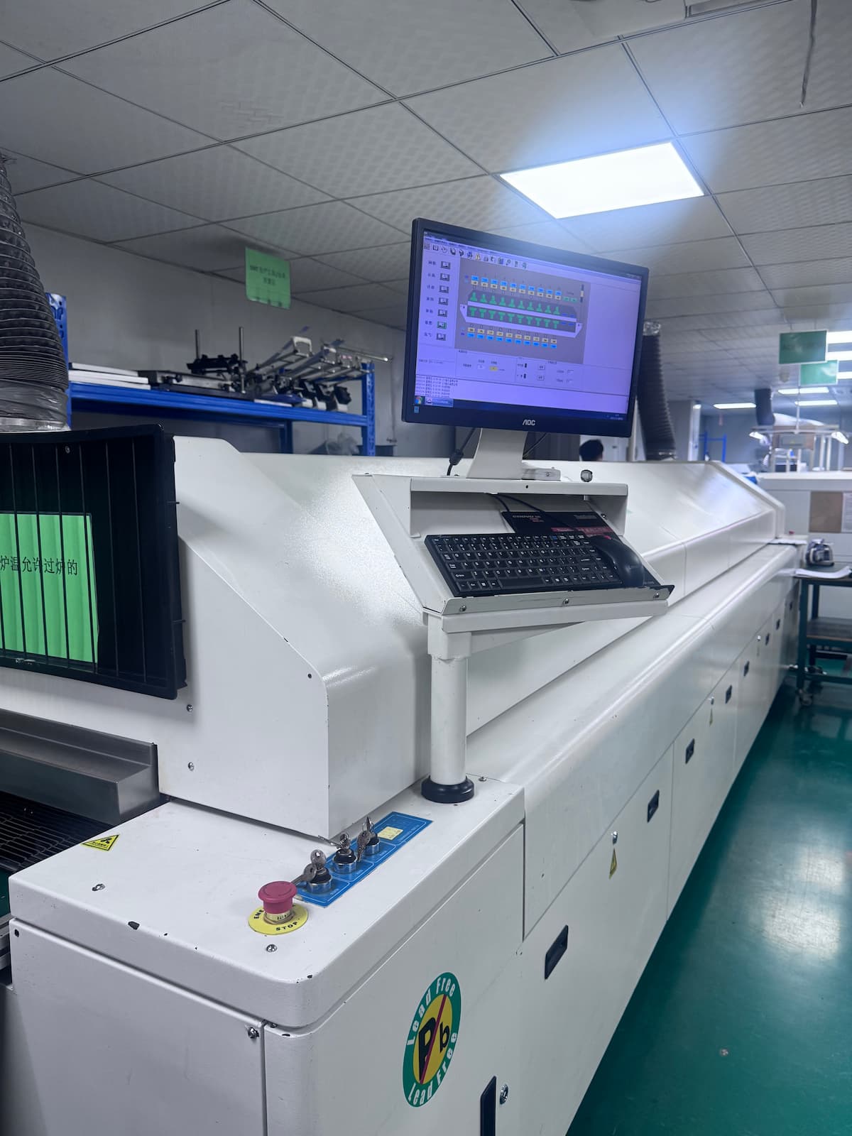
After placement, the board enters a multi-zone reflow oven. The board passes through preheat, soak, reflow, and cooling zones, each held at a precisely controlled temperature. As the board reaches peak temperature (typically around 245°C for lead-free solder), the solder paste melts and forms a permanent metallurgical bond between the component leads and the PCB pads.
Reflow profiles are tuned to the specific solder paste, component thermal mass, and board material — Linked Electronics Co., Limited adjusts the profile for each customer's BOM, especially for boards with mixed thermal masses such as heavy copper power boards with delicate ICs.
Step 5 — Through-Hole Assembly (When Required)
Many PCBAs are pure SMT, but some boards include through-hole components — large connectors, transformers, electrolytic capacitors, or relays that don't have practical SMT equivalents. These components are inserted (manually or via auto-insertion machines) after reflow, then soldered either with wave soldering, selective soldering, or hand soldering depending on volume and density.
Linked Electronics Co., Limited supports all three through-hole soldering methods, and our engineers will recommend the right approach during DFM review based on volume, component mix, and cost targets.
Step 6 — Inspection: AOI and X-Ray
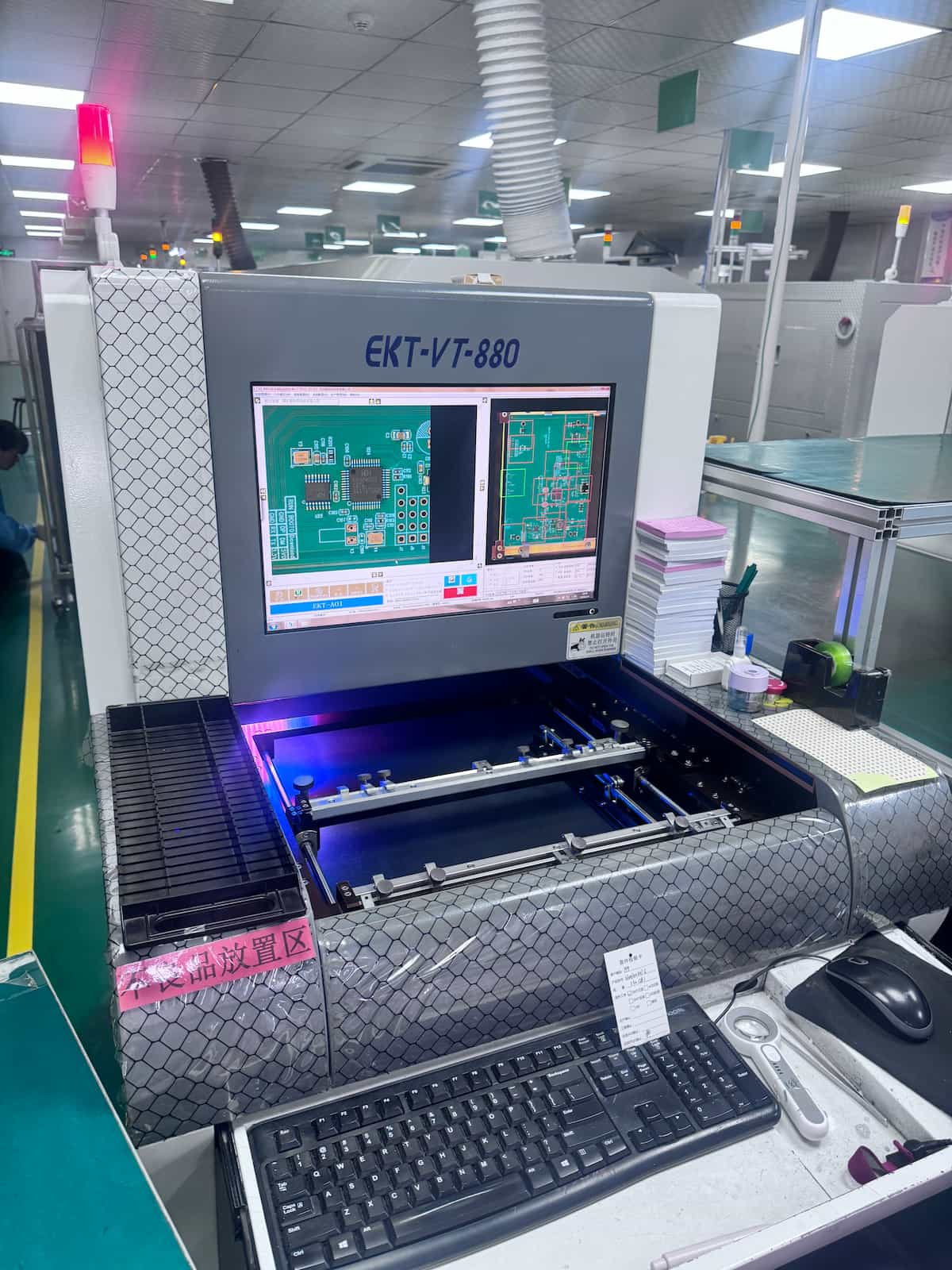
Once soldering is complete, every board passes through Automated Optical Inspection (AOI). High-resolution cameras photograph each component placement and compare it to a golden image — checking for missing components, wrong components, incorrect polarity, misalignment, and visible solder defects like insufficient paste or bridging.
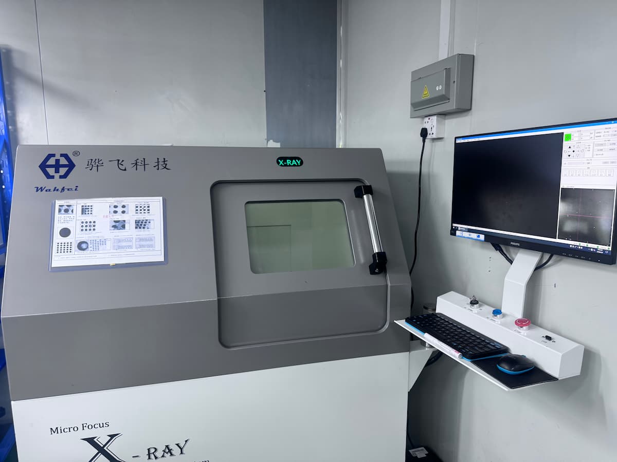
For boards containing BGA, QFN, LGA, or other bottom-terminated components, AOI is not enough — the solder joints are physically hidden under the component body. Linked Electronics Co., Limited uses 2D and 3D X-Ray inspection to verify solder joint integrity beneath every BGA, detecting voids, bridges, and head-in-pillow defects that would otherwise reach the customer undetected.
Step 7 — Functional Testing and Final QC
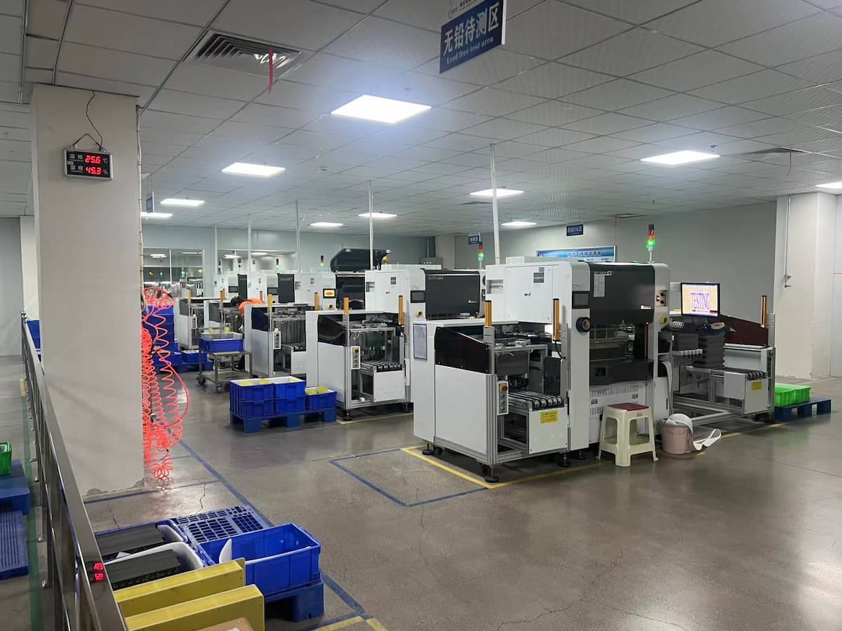
The final stage verifies the PCBA actually works. Depending on the project, this can include:
- In-Circuit Test (ICT) for high volumes (fixture-based, fast)
- Flying probe testing for prototypes and low volumes (no fixture required)
- Customer-supplied functional test fixtures executing the board's actual firmware
- Burn-in and environmental testing for automotive and medical-grade products
Linked Electronics Co., Limited owns flying probe testers in-house, allowing us to electrically verify prototype PCBAs without requiring the customer to design and fund a dedicated test fixture. For mass production, we work with customers to integrate ICT and functional test stations directly into the assembly line.
Common PCBA Questions
What is the minimum component size you can place?
Linked Electronics Co., Limited's SMT lines routinely place 0201 (0.6×0.3 mm) chip components, the smallest size in mainstream production. 01005 components are possible on request but require specific solder paste and stencil considerations.
Can you assemble BGA packages?
Yes. We assemble BGAs down to 0.3 mm pitch and inspect every BGA assembly with X-Ray. We have extensive experience with FPGAs, SoCs, and memory packages requiring tight registration and void control.
Do you offer turnkey PCBA, or only consigned assembly?
Both. Turnkey is the most common — Linked Electronics Co., Limited sources every component on the BOM from authorized distributors (DigiKey, Mouser, Arrow, Avnet, Future Electronics, Element14) and presents one consolidated quote. For customers with existing component inventory or special part requirements, we also support consigned assembly where the customer supplies all or part of the BOM.
What's your minimum order quantity (MOQ) for PCBA?
There is no fixed MOQ. We assemble single-piece prototypes for engineering verification, low-volume production runs of 50–500 boards, and mass production runs of 10,000+ pieces. The same SMT line and quality systems serve all volume tiers.
How long does PCBA typically take?
Standard PCBA turnaround at Linked Electronics Co., Limited is 7–10 business days after component arrival, but expedited builds in 3–5 days are available for prototypes. The longest lead time is usually component procurement, not assembly itself — DFM review and quoting are completed in 24 hours.
Do you support IPC Class 2 and Class 3 workmanship?
Yes. Linked Electronics Co., Limited's standard production targets IPC-A-610 Class 2. Class 3 (high-reliability, used in aerospace, medical, and automotive applications) is available on request — it requires tighter process controls, more rigorous inspection, and is priced accordingly.
Why Customers Choose Linked Electronics Co., Limited for PCBA
- In-house PCB fabrication and PCBA assembly under one roof — no coordination overhead between separate vendors
- Complete SMT line including solder paste printer, high-speed pick and place, multi-zone reflow oven, SMT AOI, and 2D/3D X-Ray inspection
- IATF 16949 quality system, RoHS and REACH compliant, with full Conflict Minerals declaration
- Authorized component sourcing from DigiKey, Mouser, Arrow, Avnet, Future Electronics, and Element14
- 24-hour DFM review and quoting on submitted Gerber files
- NDA-protected design files — your Gerber and BOM are never shared
- Prototype to mass production on the same line — no requalification when scaling
Ready to Quote Your PCBA?
Send your Gerber files, BOM, and assembly notes to [email protected] for a 24-hour turnkey PCBA quote from Linked Electronics Co., Limited.